A Better SVF Preamp – Let's get Physical
Posted
After yet another long period of radio silence, I'm back with an update on my digression into analog audio processing. So no programming again, sorry. But this time, we move from the theoretical realm of analog electronics to the physical implementation! Sounds interesting? Then read on!
First, let's look into a small modification to our circuit. In the previous post, I mentioned that to adapt the wide-bandwidth polyphonic pickups that I plan to use, we'll need a filter to adjust the bandwidth and a summing amplifier to make the signal monophonic when using them with a standard amp instead of a true polyphonic setup. However, since an SVF already requires three op-amps, adding a fourth in an inverting unity gain setup just to get a virtual ground summing node seems quite wasteful and power hungry, and you really want your 9V battery to last for more than a few dozen hours. But we don't actually need to do that! Remember how we used the fact that the inverting input of the second and third stage approximates a virtual ground? Well, so does the inverting input of the first stage to which the input is connected! So instead of one input with one input resistor to set the input impedance (below the resonant frequency, at least), we can just use n inputs with n input resistors and get virtual ground summing for free!
Is that all we need to change to turn the schematic from last time into a real-world circuit? Of course not! What do we need? Let's see, we need to…
- select an op-amp;
- connect the circuit to the outside world, so we'll need some connectors;
- power the circuit off a single battery (or phantom power—more on that later), so we have to use AC coupling capacitors and generate a half supply voltage “ground” since we won't have dual positive and negative supply voltages;
- filter the power supply voltages, as real-world batteries are not ideal voltage sources;
- add supply decoupling caps near the op-amp's power pins, since every wire or PCB trace has a parasitic inductance which can cause trouble when a fast op-amp tries to suddenly draw more current;
- add reverse voltage protection to prevent accidents from immediately destroying the circuit.
Oof, that's a lot. So let's fire up KiCAD 6 and get started! At this point, I should mention that I haven't really done any electronics work in more than a decade, so I had to learn KiCAD first, so don't expect perfection. In any case, here's the resulting schematic (sorry for the size, you can click on the image and open it in a new tab):
Regarding op-amp selection, I decided to go with the OPA1692, a low-power, low-noise, low-distortion, unity-gain stable, rail-to-rail op-amp. At only 650 μA per op-amp, the whole circuit should only draw about 2.6 mA, which is not great, but not terrible either. However, like most modern integrated circuits, it is only available as a surface mount component, so breadboarding is pretty much out of the question. So we'll have to design a PCB straight away 😱. But one nice thing that happened in the past decade: there are now some very inexpensive PCB manufacturers and per-via charges that I was used to from before are gone too!
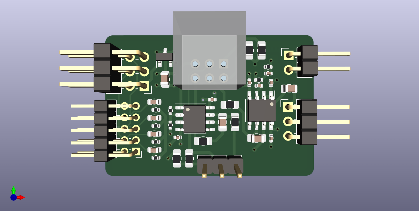
J1 is a 2 mm pitch pin header, as that's what Cycfi use to connect their polyphonic pickups. Pins 7 to 10 are not connected, as my bass has four strings, so the remaining four channels are unused anyway. For all other connectors, I used 2.54 mm (100 mil) pitch pin headers, since those are more common, easier to crimp with the tools that I have, and other solderless guitar pickup systems use them as well. J2 is used to pass through the signals to my balanced output board that can provide phantom power (Vph) when in use, so that the battery isn't drained unnecessarily. J3 goes to a TRS output jack, where a monophonic jack shorts Bat- to GND so that the battery is only used when the bass is in use. J4 is the battery connector. Finally, the resonance potentiometer RV1 is also connected via a header, not directly on the PCB, since I didn't want to mandate a fixed distance between the two potentiometers.
C1 to C4 and C7 provide AC coupling, i.e., they block any DC offsets from the in- or output while passing through AC, since we have to define our own offset Vref for single-supply operation. The size of these caps is computed based on the input impedance defined by R1 to R4 (R5 and R6 need to match to get unity gain in the pass-band) or the expected input impedance. However, since I'm using multi-layer ceramic capacitors that suffer from DC de-rating, i.e., their capacitance drops the more DC voltage is applied, often up to 80% near their maximum voltage, I used somewhat overdimensioned coupling capacitors. See https://weblib.samsungsem.com/mlcc/mlcc-ec.do for de-rating curves of a variety of capacitors (select the “DC Bias” curve).
U2A, i.e., one half of the second dual-channel op-amp, buffers the half supply voltage generated by R14/R15, to create a low-impedance single-supply voltage reference. The buffer is necessary as the impedance at all the Vref nodes leading to the potentiometers, i.e., at R7, R12, and R13, can be quite low. C15 is much larger than the largest capacitance the OPA1692 can drive, but since Vref is DC it shouldn't cause issues and should in fact improve the performance at high frequencies. At least it does in simulation, but if it turns out to be an issue, the part can always just be omitted.
Power supply filtering and supply decoupling is provided by C8 to C12. C8 is the main filtering capacitor. The smaller capacitors C9 to C12 are the supply decoupling caps that should be directly next to the op-amp package's V+ and V- pins. The latter is of course connected to GND since we're using a single supply, but a decoupling capacitor to VCC here certainly doesn't hurt, although it isn't strictly necessary either.
Finally, D1 is a dual Schottky diode which serves the dual purpose of reverse voltage protection and stopping the phantom power supply from the polyphonic / balanced output board from driving the battery, which is potentially dangerous as well. For pure reverse polarity a MOSFET would be more efficient due to a lower voltage drop, but to get both reverse polarity protection and to stop the phantom power from driving the battery would become somewhat complex.
Aside from that short 😉 list of changes—and the switch from 50 kΩ to 100 kΩ potentiometers and corresponding changes to shaping resistors and feedback capacitors—the basic circuit is the same as before.
For the PCB design I went with tiny 0402 (1.0 mm × 0.5 mm!) and 0603 for all resistors and capacitors that I could cheaply get assembled by the PCB manufacturer. I selected larger 0805 parts with oversized hand-soldering pads for unusual values and low-tolerance components that I would solder on myself, since I am both new to SMT soldering and have somewhat shaky hands. For the PCB stackup, I decided to go with four layers since it's not significantly more expensive and should improve EMI performance, i.e., be less sensitive to picking up electromagnetic noise from the environment, due to the smaller distance between ground plane and signal traces.
The design process was tedious, positioning and repositioning components again and again until I had a layout with minimal layer changes and a small board size. I'm sure the next one will go much quicker. In any case, here's the result:

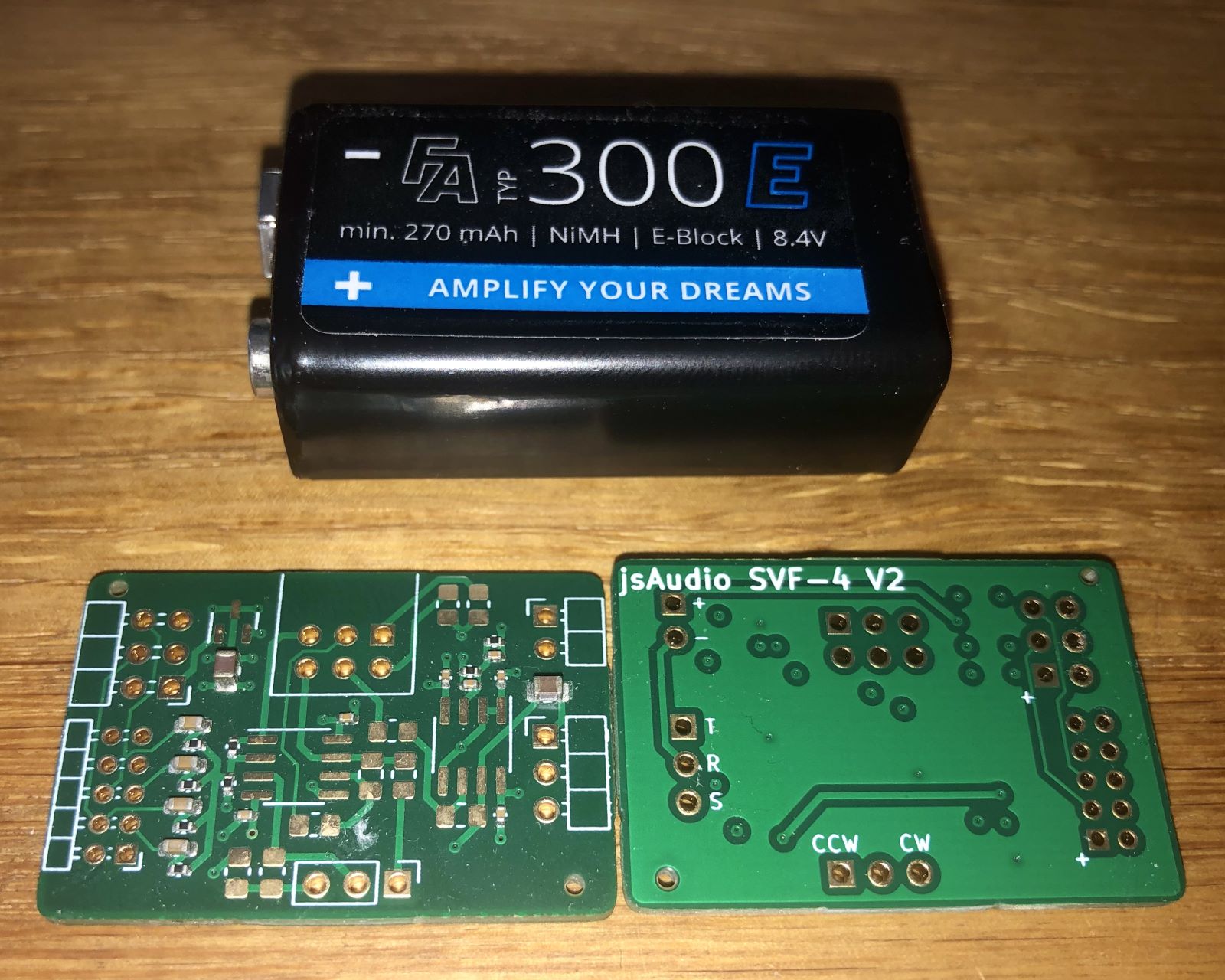
And through the magic of editing, or rather the fact that a lot of time has passed between this post and the last, here's what I received (9V battery for scale):

Why does it say “V2” on the back, I hear you ask? Well, I may or may not have accidentally swapped the inverting and non-inverting inputs of the op-amps in the first version that I submitted to the manufacturer. Another reason besides shipping times and Chinese holidays that this post is so late.
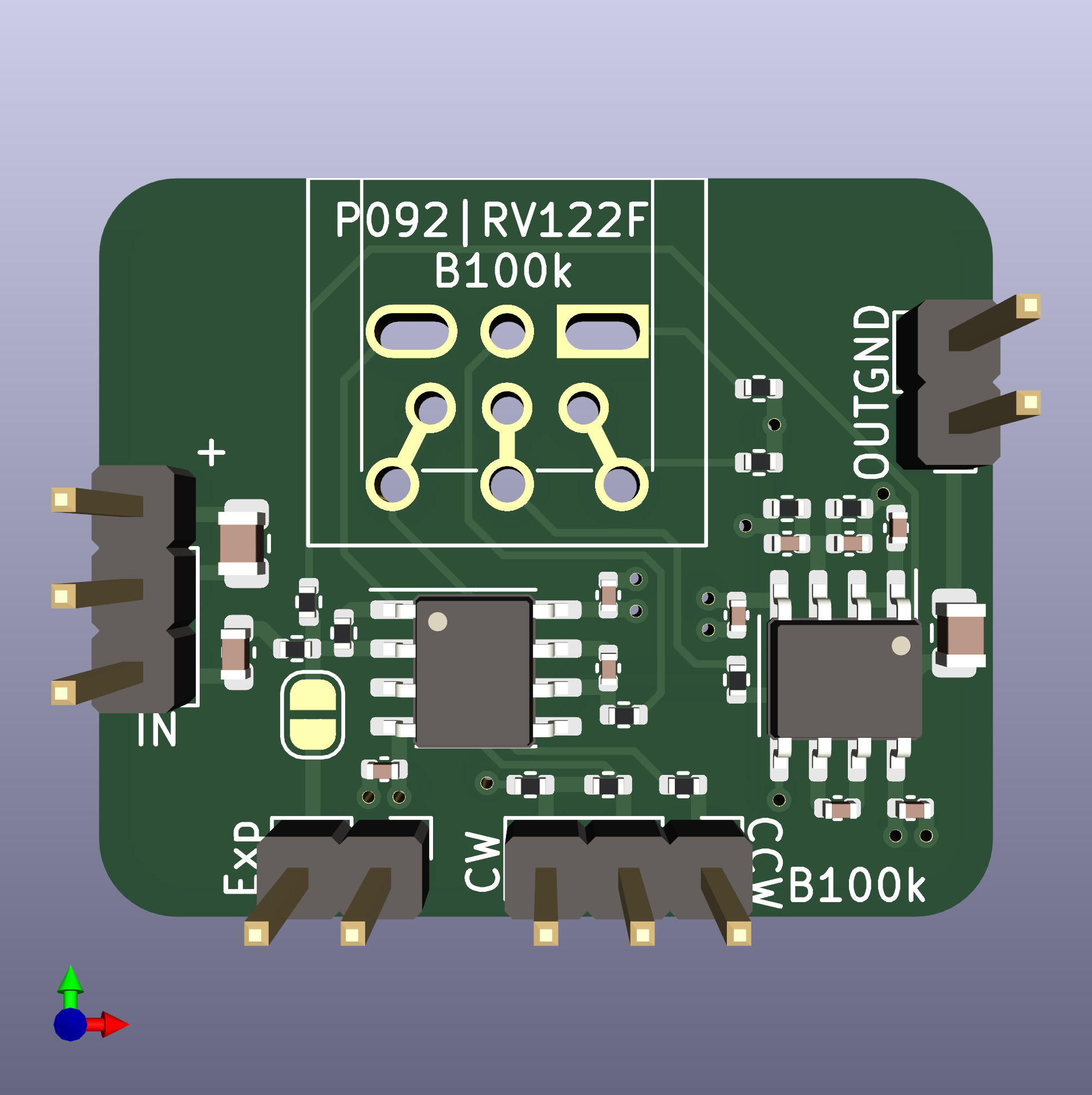
Is that it? There are still a couple improvements that can be made to the preamp that I thought of after making this first version. By adding a connector to the input summing node, the preamp could be used both with a traditional, monophonic pickup, and with polyphonic pickups with four, six, or more channels. By rounding the capacitor values (910 pF is quite close to 1 nF) differently and by selecting resistors in E12, resistors and capacitors available at the manufacturer in small sizes could be used instead, while only incurring a small error in adjustment range. They don't currently have any op-amps that match my purposes in stock and unusual parts incur an additional cost anyway, so I'll stick to hand-soldering those for future revisions too. Also, it turned out that the potentiometers I chose have fairly short threading and definitely won't fit a guitar with a wood top and not a pickguard. Not a big issue, since their 2.5 mm pitch is close enough to 2.54 mm that I can use different ones via a pin header, but it would be nice to be able to select different ones. Here's one potential work-in-progress design:

That's it for this post. No proper sound samples yet, as I'd need to do some custom routing (and lack a router of the woodworking kind) to get everything into the bass. Also, my first SMT soldering job looks so bad that I don't want to show you a picture of that 😅. As per usual, feel free to follow me and send me a DM on Mastodon if you have any questions or comments.
